


Silicon Carbide Electronics and Sensors
NASA is developing silicon carbide technology to enable smart electronics in extreme conditions, boosting performance in aerospace, power, auto, and energy sectors.
Overview
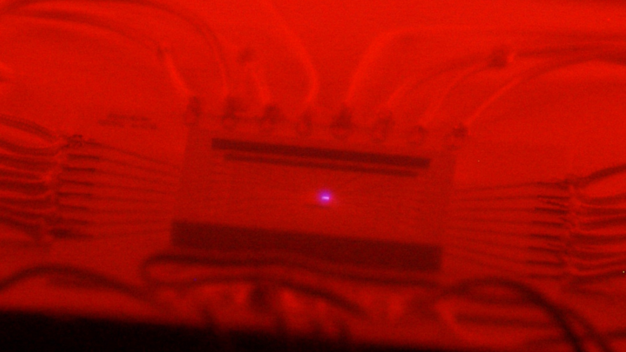
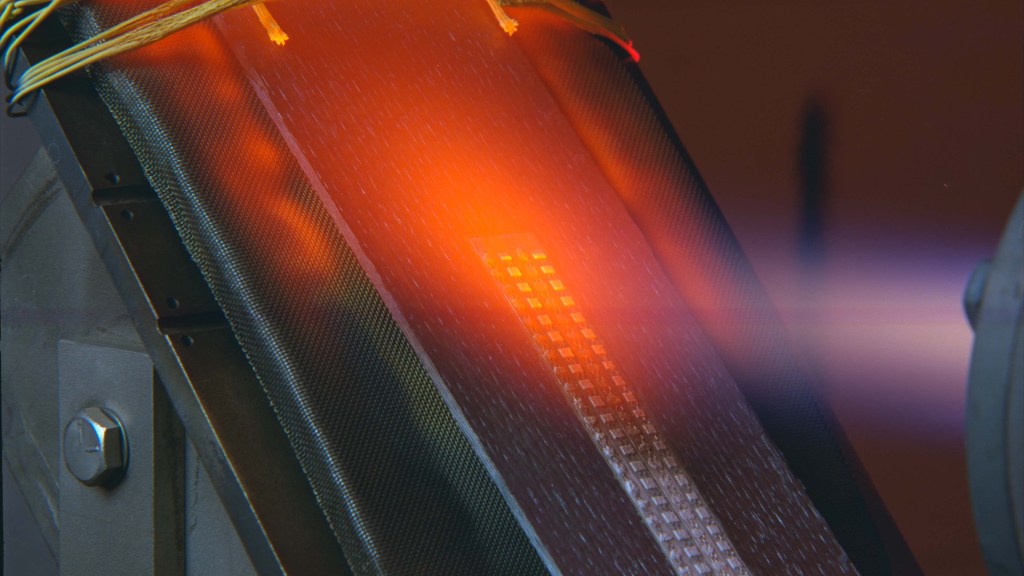
NASA’s Glenn Research Center in Cleveland is developing silicon carbide (SiC) to enable intelligent sensing and control electronic subsystems into extreme aerospace (including 600°C [1,112°F]—hot enough to glow red!) that are beyond the physical capabilities of conventional silicon technologies. Silicon carbide’s ability to function in high temperature, high power, and high radiation conditions enables important performance enhancements across aircraft, spacecraft, power, automotive, communications, and energy production industries.
SiC Research at NASA Glenn
NASA Glenn continues to build on its pioneering SiC electronics history, dating back to the growth of single-crystal layers that formed the basis of early SiC diode and transistor demonstrations. NASA Glenn’s advancements in SiC technology helped establish today’s global SiC wafer and power device industry for conventional applications (typically under 200°C)
Work With NASA Glenn SiC Technology
Could your system benefit from long-duration sensors and integrated circuits (IC) capable of operating in extreme environments?
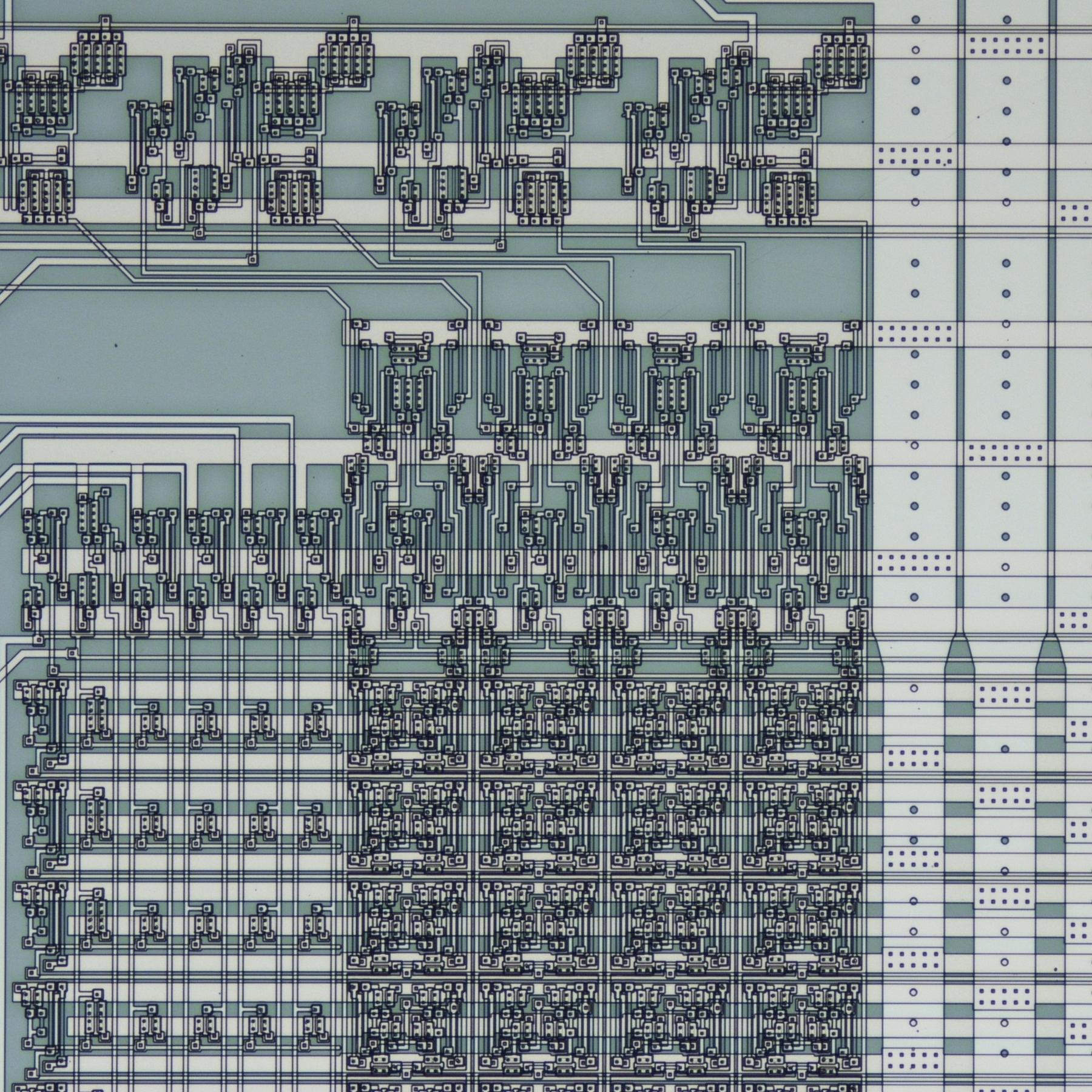
Recognizing the importance of accessibility and commercialization for technology infusion, NASA Glenn prototypes developmental SiC IC designs for interested external partners and is exploring a transition to commercial wafer foundries. The NASA Glenn 500°C Durable Junction Field-Effect Transistor Technical User Guide aims to inspire exploratory design, simulation, and layout of application-specific SiC ICs by new technology users.
This guide enables qualified electrical engineers to design SiC ICs for potential inclusion in future developmental fabrication runs at NASA Glenn.
To explore partnership or licensing opportunities for NASA Glenn’s SiC electronics and sensors, please contact Jeanne King at the NASA Glenn Research Center Technology Transfer Office (jeanne.m.king@nasa.gov, 216-433-2095).
Glenn Discoveries
NASA Glenn has long been a leading driver of SiC technology, as it was one of the first U.S. government agencies to fund and carry out SiC research work. The core SiC research team was founded around 1980 by NASA Glenn Hall of Fame inductee J. Anthony Powell. Over the years, NASA Glenn research team has contributed several significant discoveries to the emerging high-technology silicon carbide field. These discoveries include the following
- First large-area epitaxial growth of silicon carbide on silicon wafers (1982).
- First kilovolt (1991) and multi-kilovolt (1993) SiC rectifier devices.
- Site competition effect widely utilized for SiC dopant control (1993).
- Identification of micropipes as crystal defects that limit the performance of SiC power devices (1993).
- First semiconductor logic gate operation at 600°C (1996)
- First SiC ohmic contacts stable for 1000 hours at 600°C in air (2000).
- First Semiconductor Integrated Circuits to Operate for Thousands of Hours at 500°C (2007).
- First Electronics to Function for Weeks in Venus Surface Atmospheric Conditions (2016).
- First Semiconductor Integrated Circuits to Operate Above 900°C (2017).
- First Medium-Scale Integrated Circuits to Operate Over a Year at 500°C (2018).
Sponsored Offsite SiC Research
NASA Glenn sponsored research (through contracts to industry and grants to universities) has also resulted in several pioneering advancements in silicon carbide technology. For example, NASA Glenn sponsored the early stages of SiC power MOSFET development at Cree in the early 1990’s under NASA Small Business Innovative Research (SBIR) program. Cree/Wolfspeed is now recognized as one of the world’s leading manufacturers of SiC power MOSFETs that are enabling higher-efficiency power conversion and management circuits.
Today, NASA Glenn remains in a unique position to make crucial advancements to silicon carbide technology. The continuing importance and relevance of NASA Glenn SiC research is reflected in the strong support of our research customers and collaborators. The NASA Glenn SiC team is also collaborating with the NASA Glenn Chemical Sensors team towards developing hostile-environment SiC-based gas sensors.
Explore This Area Further

Benefits and Collaborations
The benefits of silicon carbide (SiC) electronics and sensors can extend to spacecraft, aircraft, power, automotive, energy production, and communications. These have resulted in collaborations with industry, universities, and other government agencies.
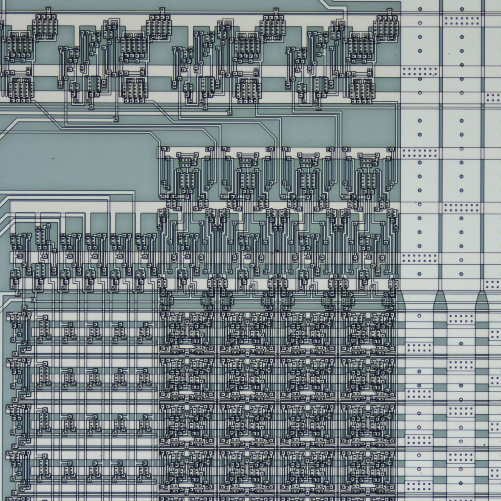
Junction Field-Effect Transistor Integrated Circuit Technical Guide
This guide stimulates further exploratory design, simulation, and layout of potentially beneficial application-specific JFET-R ICs by new potential technology users.
NASA Glenn facilities where this research is conducted:
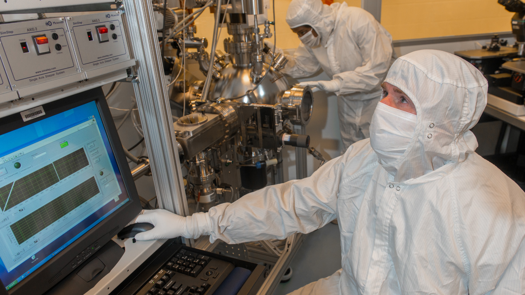
Microsystems Fabrication Laboratory
This vertically integrated silicon carbide (SiC) semiconductor research and development facility is dedicated to the design, fabrication, and testing of integrated circuit electronics and sensors uniquely durable to extreme environments.
Learn More about Microsystems Fabrication Laboratory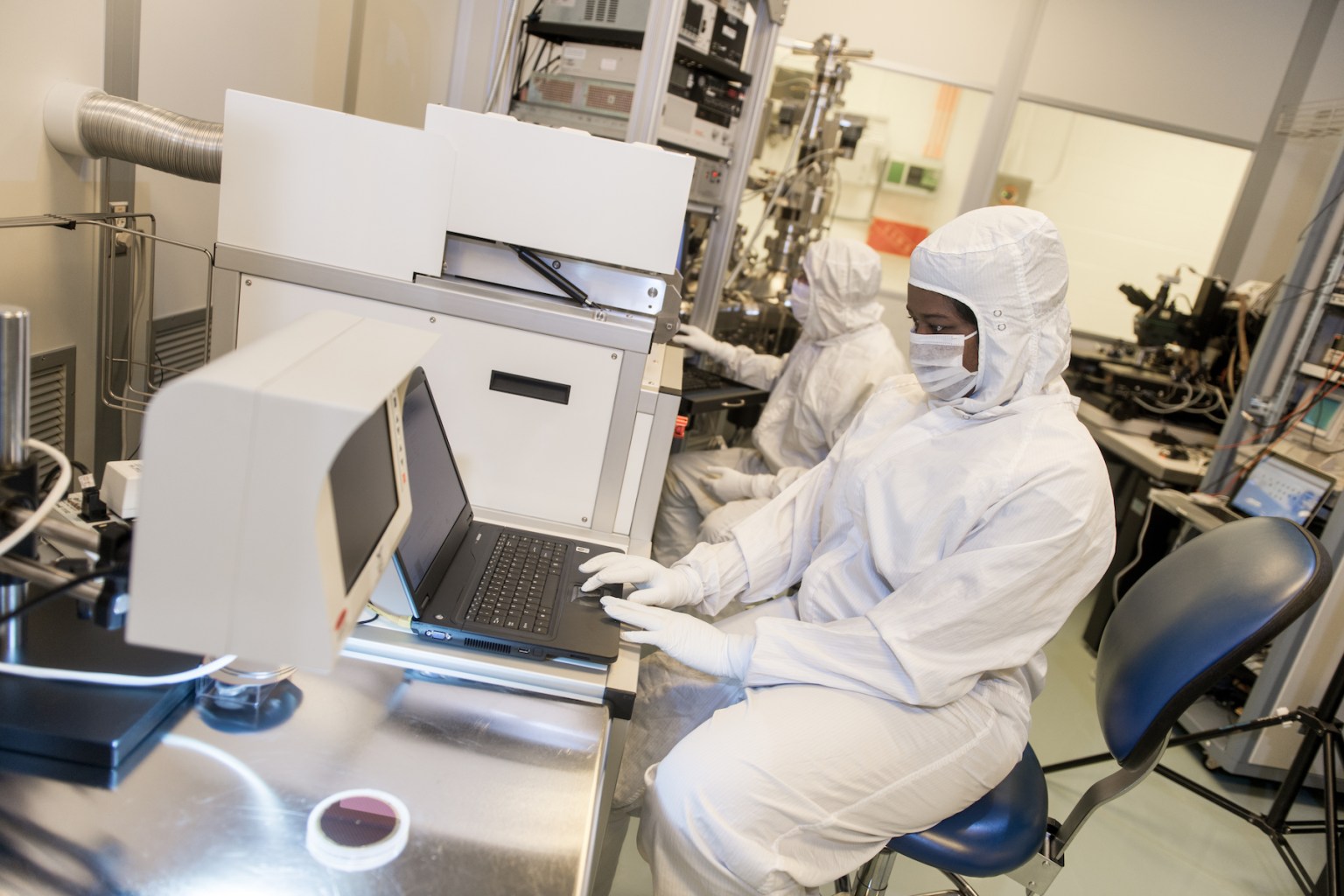
Publications
Use the search feature to filter publications data across all columns.
Details
Patents
Use the search feature to filter patents data across all columns.
Details
Contact
| Area of Expertise | Name | |
|---|---|---|
| Technical Lead | Gary Hunter | gary.w.hunter@nasa.gov |
| SiC Transistors and Integrated Circuits | Philip Neudeck | neudeck@nasa.gov |
| SiC Sensors and Microelectromechanical Systems (MEMS) | Robert Okojie | robert.s.okojie@nasa.gov |
| SiC Device Fabrication | Shamir Maldonado-Rivera | shamir.maldonado-rivera@nasa.gov |
| SiC Device Fabrication | Srihari Rajgopal | srihari.rajgopal@nasa.gov |
| SiC Device Fabrication | David Spry | david.j.spry@nasa.gov |
| SiC Circuit Design | Mike Krasowski | michael.j.krasowski@nasa.gov |
| SiC Circuit Design | Norman Prokop | norman.f.prokop@nasa.gov |
| SiC Circuit Design and Testing | Christina Adams | christina.m.adams@nasa.gov |
Discover More Topics From NASA
Sensors and electronics research at NASA's Glenn Research Center
Advanced Space Radiation Detectors
NASA is developing low-noise, robust, compact radiation detectors to provide improved data on space radiation.

Chemical Sensors
NASA is developing chemical species sensors for aerospace applications including leak detection and emission, safety, human health, and environmental monitoring.
Physical Sensors
NASA is developing innovative harsh environment physical sensing and instrumentation technologies to advance next-generation space exploration, science, and aeronautics research.