


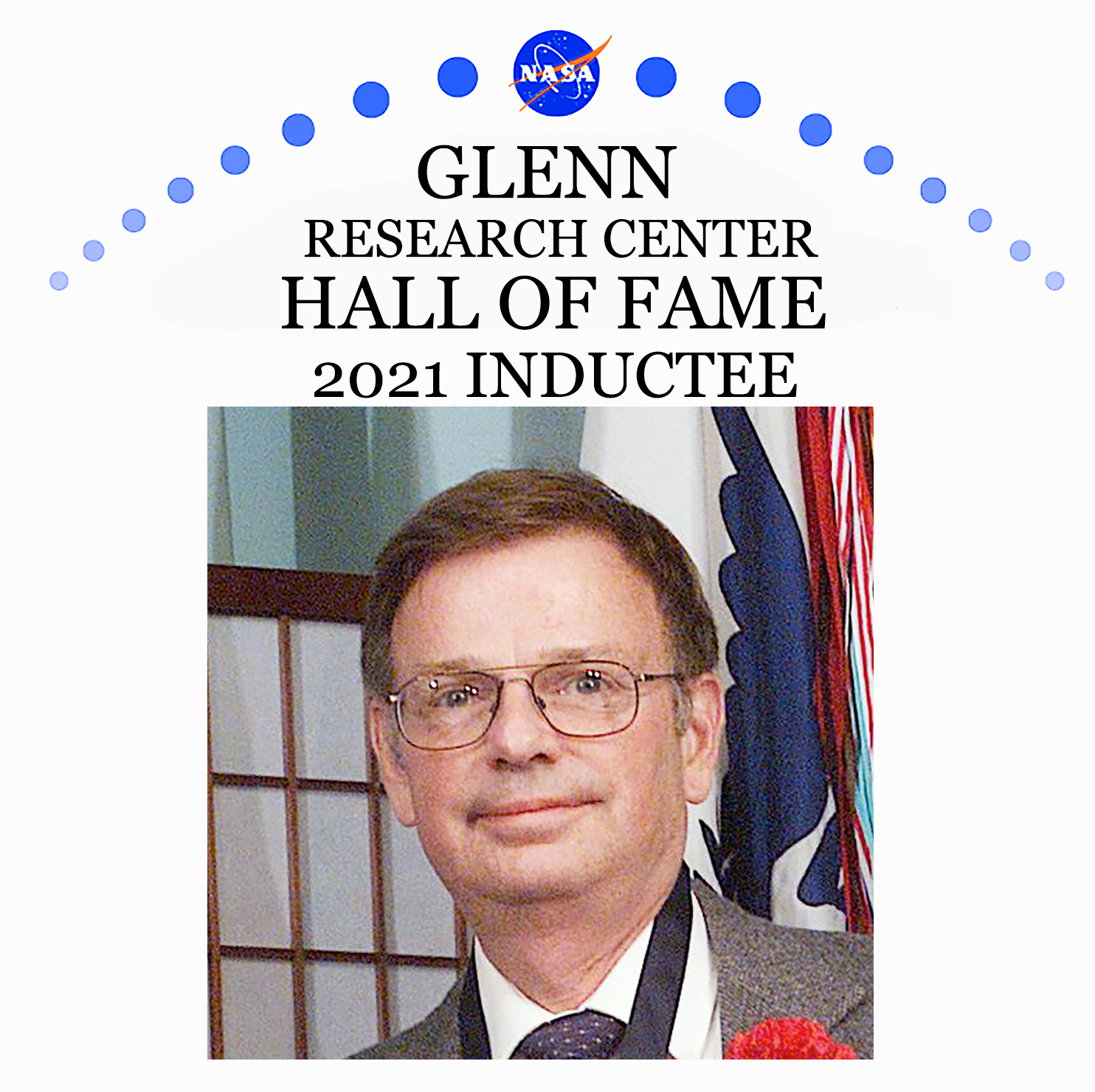
Citation
J. Anthony Powell was international recognized as a pioneering leader in the development of high-temperature electronics based on silicon carbide (SIC). He realized early on that the key to SIC-based electronics lies in the development of a viable low-dislocation substrate. Through his application of chemical vapor deposition and his subsequent improvements, Powell became the first to achieve the desired substrate. His breakthrough led to a world-class SIC electronics program at the center, the establishment of a growing multimillion-dollar commercial SIC marked, and the incorporation of SIC-based electronics in NASA’s Venus lander.
Biography
J. Anthony Powell became interested in science and engineering, particularly electronics, while growing up in Lexington, Kentucky, which was then relatively small city. He was drawn to physics while earning his undergraduate degree in electrical engineering at the University of Kentucky. A professor recognized this interest and allowed Powell to work summers in his solid-state laboratory. There Powell analyzed single calcium oxide crystals and created processing furnaces. Powell completed his master’s degree in Physics in 1963 and began looking for professional employment in Ohio, which had significantly more scientists and engineers than Kentucky.
Powell accepted a position in the Instrument Research Division at NASA’s Lewis Research Center in Cleveland, Ohio. The center was dramatically expanding its workforce as part of the agency’s effort to land a man on the Moon by the end of the decade. In September 1963 the 25 year-old Powell purchased a new car, packed just a few belongings, and headed north to start a new life.
As a member of the Measurements Section (1963 to 1965) and the Electronic Systems Section (1966-1970), Powell helped initiate the center’s research on silicon carbon crystals. Electronics using pure silicon crystals cannot meet the extreme temperature and power requirements for proposed spacecraft and supersonic aircraft.
Powell recognized that silicon carbide electronics offered significantly better electric field strength breakdown, bandgap, thermal conductivity, and higher operating temperatures than pure silicon, but there was no established process to grow silicon carbide crystals of uniform size and consistent quality.
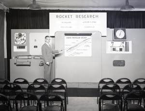
Powell explored several avenues for silicon carbide growth in the late 1960s and had some small-scale success. Despite its promise, the technology was not commercially viable without silicon carbide substrates of adequate quality and purity. Lewis cancelled the program in the early 1970s and, with the exception of the Soviet Union, nearly all silicon carbide electronics research ceased.
In 1974 Powell was assigned to the Electronic and Laser Applications Section of the Airbreathing Engines Division. The group sought to improve methods of accurately measuring the conditions inside of operating aircraft engines. Powell and his colleagues developed a laser anemometer that detected air stream particles as they passed through two intersecting laser beams. Researchers could calculate the velocity of the particles from the time and the distance data. The device could take thousands of measurements per second at the compressor’s complex set of rotating fan blades.
In 1981 Powell became a member of the Electronics and Electro-Optics Section, which was developing electronic monitoring systems for aircraft engines. Engine manufacturers required semiconductors for electronics that could function in a high-temperature environment, renewing Powell’s interest in silicon carbide. He and William Nieberding authored a report asserting that silicon carbide semiconductor electronics could significantly impact modern aircraft engines. The paper spurred the center to reinvest in silicon carbide electronics research.
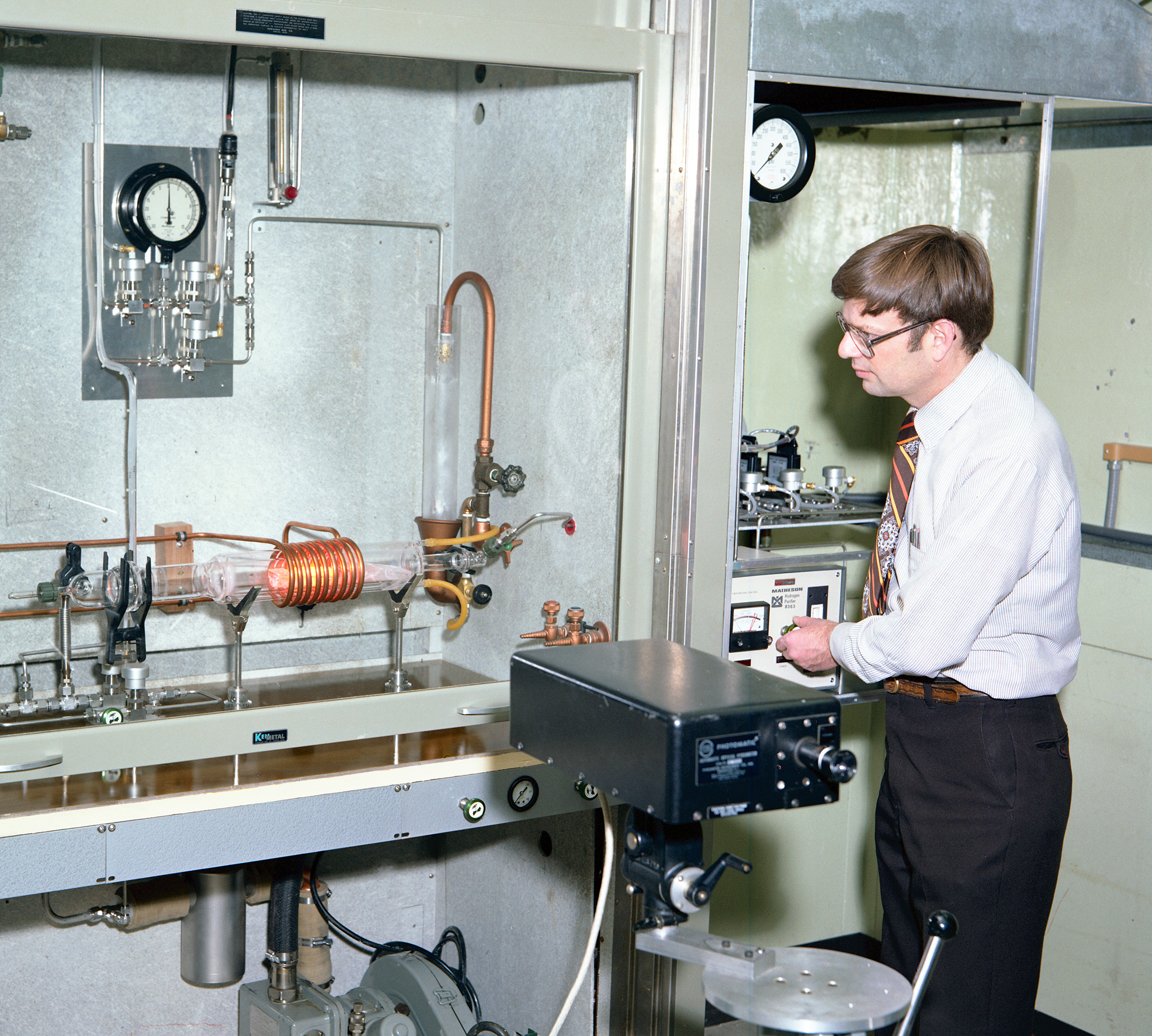
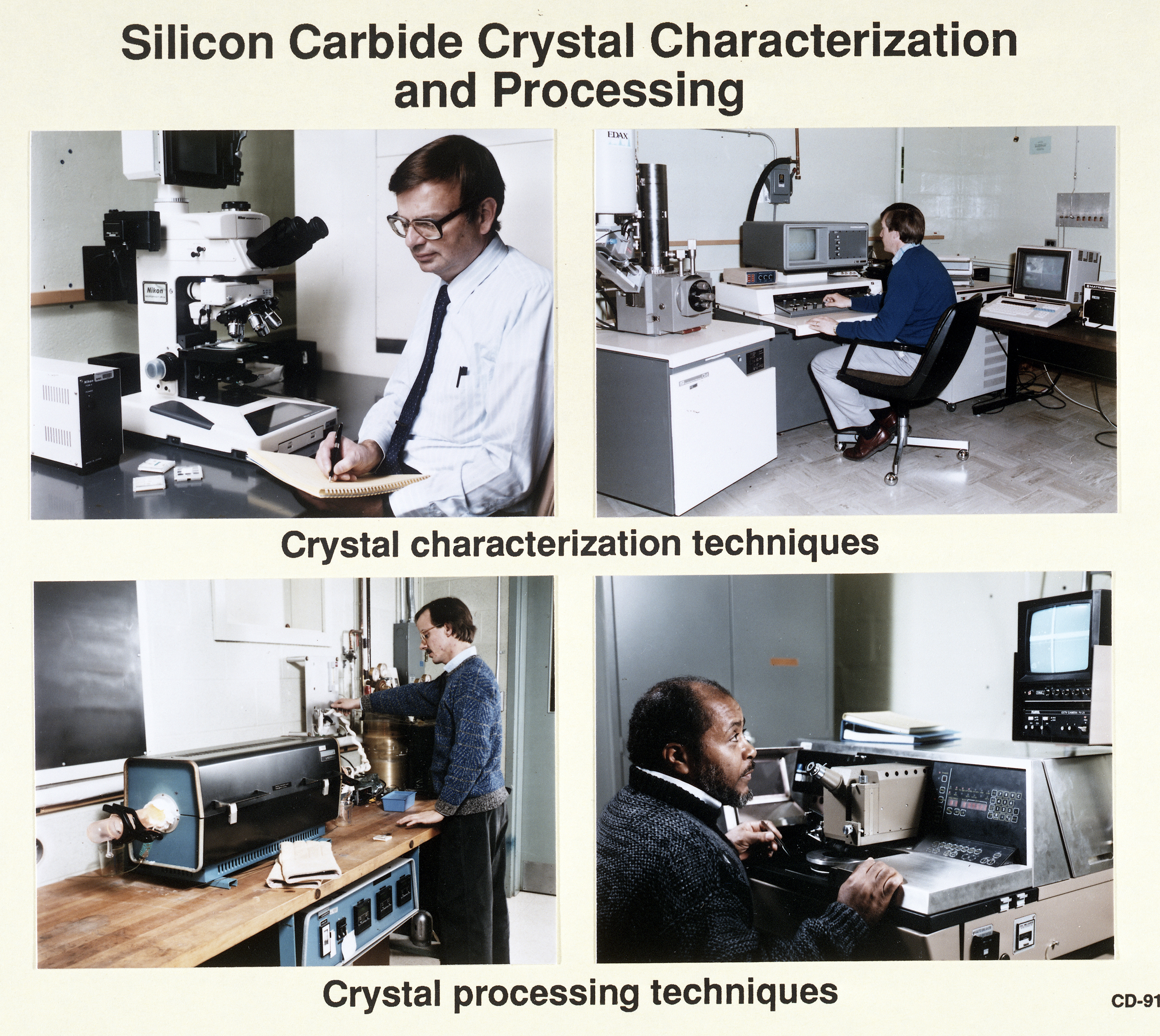
Visiting faculty fellow Dr. Shigehiro Nishino introduced the Lewis team to a unique chemical vapor deposition (CVD) strategy to grow silicon carbide crystals on silicon wafers. Powell and his colleagues constructed a laboratory to apply the CVD and successfully worked through the various processing issues. The CVD growth of high-purity silicon carbide layers would prove to be a key breakthrough that made silicon carbide electronic devices a reality. Research & Development Magazine included this process on its renowned R&D 100 list of exceptional technologies for 1983. Silicon carbide research quickly expanded around the globe.
As a member of Engine Sensor Technology Branch, Powell understood that future commercialization of silicon carbide semiconductors would require low densities of crystal defect. In the mid-1980s he partnered with regional universities to develop strategies to eliminate crystalline defects. Powell’s landmark 1989 paper on the use of CVD to grow low-defect silicon carbide layers on commercially available silicon carbide wafers paved the way for the development of high-quality silicon carbide electronic devices.
Powell’s pioneering application of CVD for silicon carbide growth is one of the technical foundations of what has blossomed into a global industry. Silicon carbide electronics are utilized by renewable energy grids, computer power supplies, nuclear power-generating systems, electric vehicles, hybrid electric aircraft, and space vehicles. The increased use of silicon carbide electronics in electrification systems has contributed to the reductions of global greenhouse emissions.
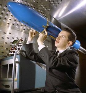
Exploration of the planet Venus has long been hampered by the inability to design equipment to survive the planet’s high temperature and pressures. In the early 1990s Powell argued that transmitters using silicon carbide electronics would survive the harsh conditions. NASA researchers have subsequently made silicon carbide a key component of the planned Long-Lived In-Situ Solar System Explorer (LLISSE) mission to Venus. The resilience of silicon carbide, predicted by Powell, has been verified by long-duration testing under simulated Venus conditions.
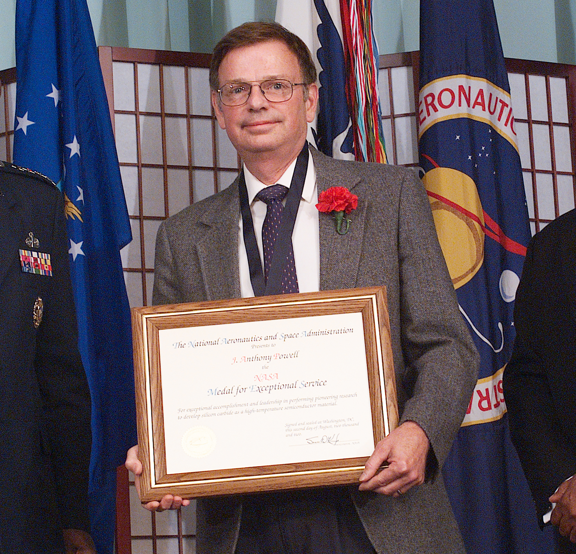
Powell published over 30 technical papers and earned several patents while at the center. NASA recognized Powell’s impact with a series of awards, including a Special Achievement Award (1973), Lewis Technical Publication of the Year (1980), Exceptional Engineering Achievement Award (1990), and Exceptional Service Award (2002). In addition, his projects were included on the IR 100 and R&D 100 lists in 1983 and 2004. He has served on steering committees, chaired numerous international conference sessions, and served as an advisor and reviewer for national research organizations.
Powell retired in the early 2000s but continued his work in the private industry. In 2012, he was a member of a team that received the NorTech Innovation Award for nearly perfecting silicon carbide manufacturing.
Despite being an internationally recognized figure, Powell remained humble and eager to learn from others. His family recalls him excitedly setting off each morning for, what he referred to as, “the best job in the world.”
Related Documents
Photographs