Jacob Boyer
The Ohio State University
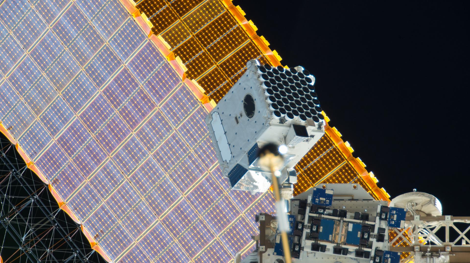
High substrate costs, as well as weight, typically play a major role in the high costs of multijunction space solar cell production and deployment. III-V/Si multijunction structures provide a potential solution to this through the use of an exceptionally inexpensive (and lightweight) substrate that also serves as an active cell component, combined with a III-V semiconductor stack tailored to space PV needs to provide high efficiency. Already, GaP/Si has been demonstrated in MBE and MOCVD growth modes, with dual junction cells for terrestrial application under development.
This proposed work seeks to generate optimized III-V/Si structures for space power generation. Using prior knowledge of terrestrial photovoltaics efforts in III-V/Si technology, my goal is to adapt these dual junction (and ultimately triple junction) devices for space deployment via tailoring the bandgaps of the III-V component(s) for optimized AM0 absorption, and addressing radiation hardness issues with silicon. With the right composition of GaAsyP1-y and (AlzGa1-z)xIn1-xP alloys on silicon, maximum efficiencies under AM0 are calculated to be ~41% and ~45% for the dual and triple junction cells respectively.
A significant part of this optimization process will involve investigation of metamorphic materials required to join the GaP lattice constant to the targeted GaAsyP1-y and (AlzGa1-z)xIn1-xP alloys, enabling the optimum composition/bandgaps for dual junction and triple junction devices. Metamorphic materials encompass many forms of crystalline defects which, above certain levels, greatly hinder device performance and effectiveness. Aside from normal characterization methods, including: photoluminescence spectroscopy (PL), Hall mobility, high-resolution triple-axis X-ray diffraction (XRD), and transport measurements (I-V, C-V, etc.), I will use a novel characterization technique, electron channeling contrast imaging (ECCI), to quantify defect populations and behaviors within these metamorphic materials. This work, being traditionally performed in plan-view TEM, will be significantly expedited due to the use of ECCI, which requires minimal sample preparation and avoids destroying a device. Thus, it will allow a less hindered development of defect mitigated metamorphic materials, allowing devices to more closely approach their theoretical efficiencies.
A supporting task of this research will also be to optimize the GaP/Si bottom cell for space deployment. Radiation hardness remains an issue, though I will investigate the potential benefits and demerits of utilizing thin-Si to mitigate these issues. Radiation studies will be used to understand how to design the Si bottom cell around these potential problems.
Another part of this research will be focused on device growth via MBE and MOCVD, first demonstrating space-optimized dual junction III-V/Si cells, and later developing triple junction cells. Holistic device design will be guided by physics-based modeling using technology computer aided design (TCAD) software. Individual components and entire devices will be modeled using up-to-date empirical materials properties data, dislocation aspects garnered from the metamorphic material characterization, and full testing results (e.g. DIV, LIV, QE, etc.) in an iterative developmental cycle, resulting in the realization of dual and triple junction III-V/Si photovoltaics optimized to efficiently generate solar power in space, while keeping costs of production and deployment low.


